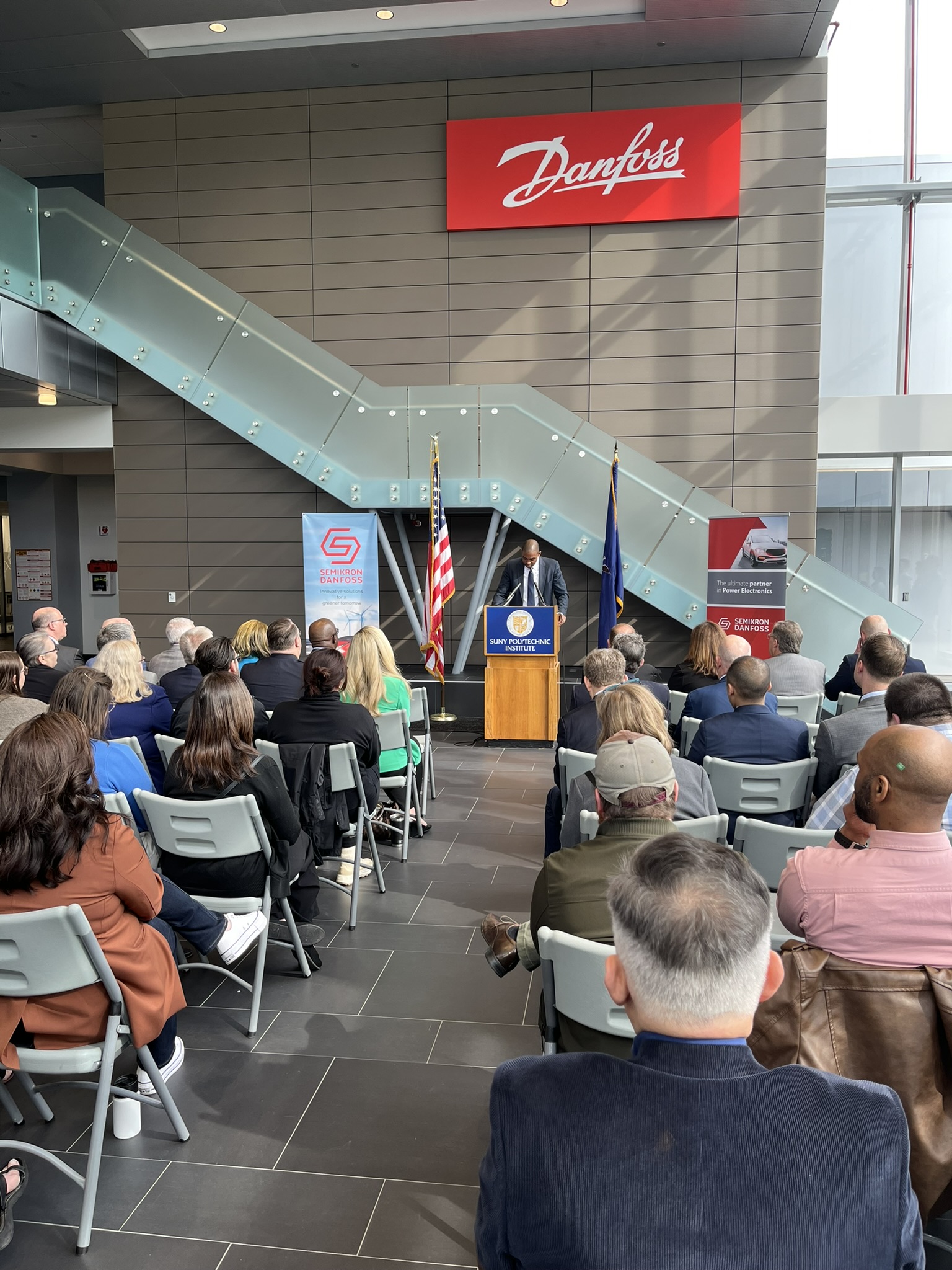
A $4M ESD grant will help fund facility in Danfoss for research and workforce development
Semikron Danfoss is excited to announce its collaboration with SUNY Polytechnic Institute and other industry partners to build a Semiconductor Processing to Packaging Center that will focus on research, education and training. The facility will be established at the Semikron Danfoss office, located in the Quad C building on the SUNY Poly campus and will train 100-150 students per year in semiconductor processing, packaging and testing capabilities.
The official announcement came on Tuesday at the site of the future facility at a ceremony attended by over 100 people, including New York’s Lt. Gov. Antonio Delgado and other state and local business leaders and elected officials. “The cornerstone of our regional economic development process is collaborative, community-led projects that will build a stronger future for New Yorkers statewide,” said Delgado.
The center will be funded in part with the $4 million Empire State Development grant, announced Tuesday, as well as a larger economic development package announced by New York Governor Kathy Hochul for SUNY Poly last fall. In addition to supplying space for two classrooms and a 5,000 square-foot clean room, Danfoss will provide multiple pieces of equipment used in the semiconductor manufacturing process.
The Center will allow for both silicon device processing as well as SiC, GaN, AlN and their alloys, and Ga2O3 device processing for power electronics, optoelectronics and clean energy applications as well as their unique packaging needs.
It is anticipated that the students will be both traditional and non-traditional students, seeking either degrees or certificates. The goal of the Center is to increase graduates across advanced manufacturing disciplines by 10 percent in the next four years. The Center’s curriculum will offer several workforce development training and upskilling pathways for industry partners and their employees as well as those seeking to gain entrance into the workforce.
“The creation of a single center covering research, education and training capabilities across semiconductor processing to packaging will provide students and the future workforce with both the deep theoretical knowledge as well as the hands-on experience needed to fully understand the workflow and attention to detail needed to produce devices with the required yield and performance functionality,” said Michael Carpenter, Ph.D., Interim Dean of SUNY Poly’s College of Engineering and Associate Provost for Research. “We are looking forward to working with Danfoss and our other industry and community partners on this initiative.”

“Partnering with educational and community organizations in the communities where we operate is an important focus of Danfoss’ mission. We are excited to work with SUNY Poly to develop a skilled workforce in the semiconductor industry.”
